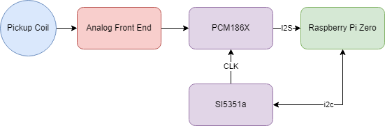
With the board assembled and the filter issues figured out the next step is to figure out the digitization process. For this we’re using a PCM186X family of audio analog converters which relies on utilizing the I2S protocol. In addition to the PCM186X device I’ve also got a SI5351a frequency generator in order to have fine control of our sampling rate. Overall the connectivity is shown below.
One important thing to note is that we are utilizing the PCM186X in master mode whereas the Raspberry Pi Zero I2S is in slave mode. This allows us to use a more accurate clock source than what is available on the pi.
Setup
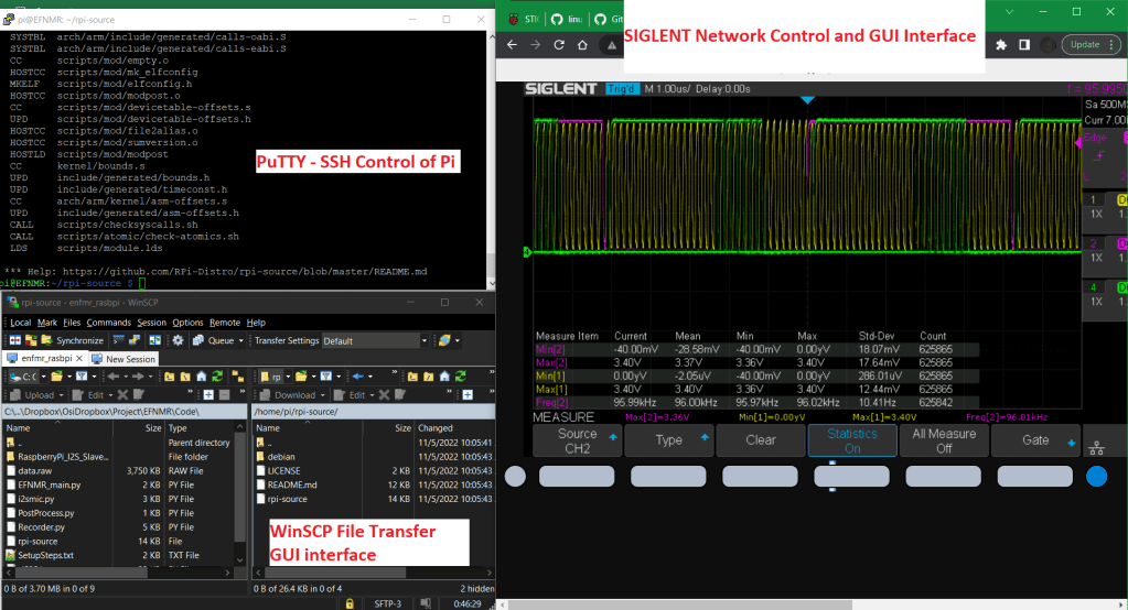
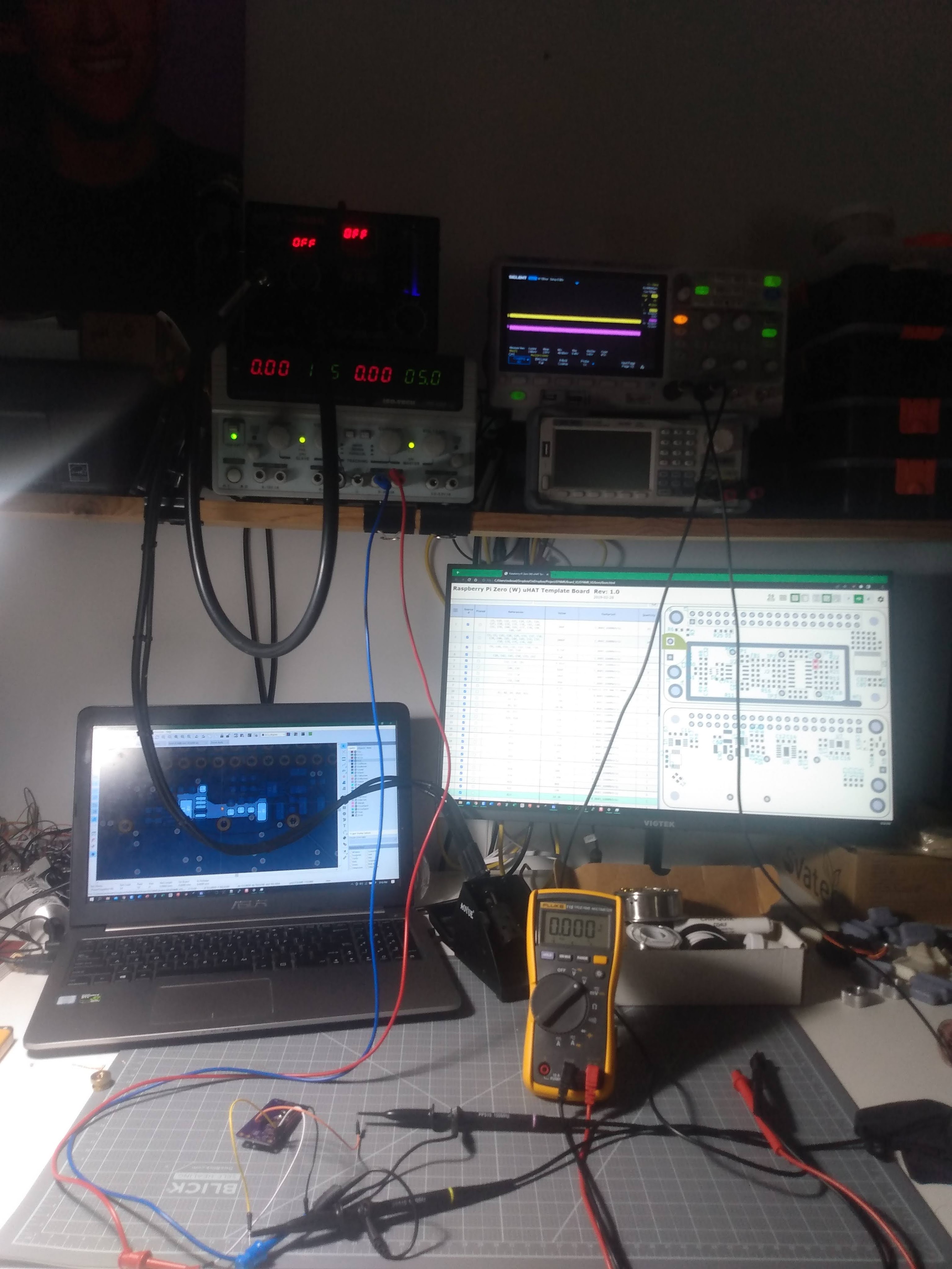
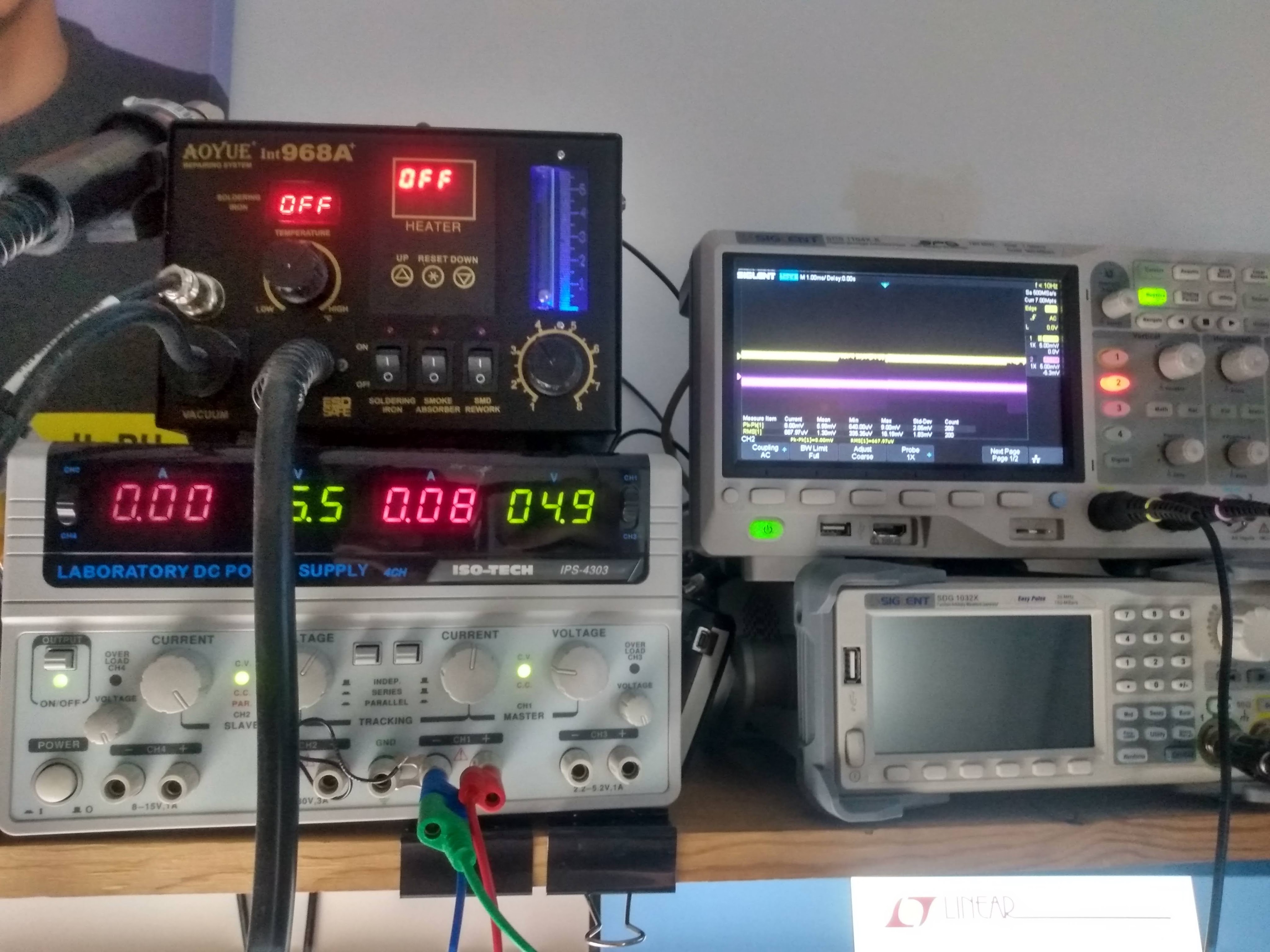
I used to be more of a bare-metal microcontroller guy, but I’m starting to really enjoy the flexibility of utilizing a single board computer running linux. The greatest thing about it is that remotely managing my devices is verrrrry easy! I can sit on my couch while my pi and scope sit on the bench in the other room. Some of the tools that I employ include PuTTY, WinSCP, and my scopes over-the-network control functionality.
SI5351a
The SI535a is a very easy to use frequency generator and is basically a 25 or 27 MHz crystal with a PLL and fractional divider. I started with using the adafruit si5351a library however modified it so that I could specify a 27MHz crystal rather than the 25MHz crystal.
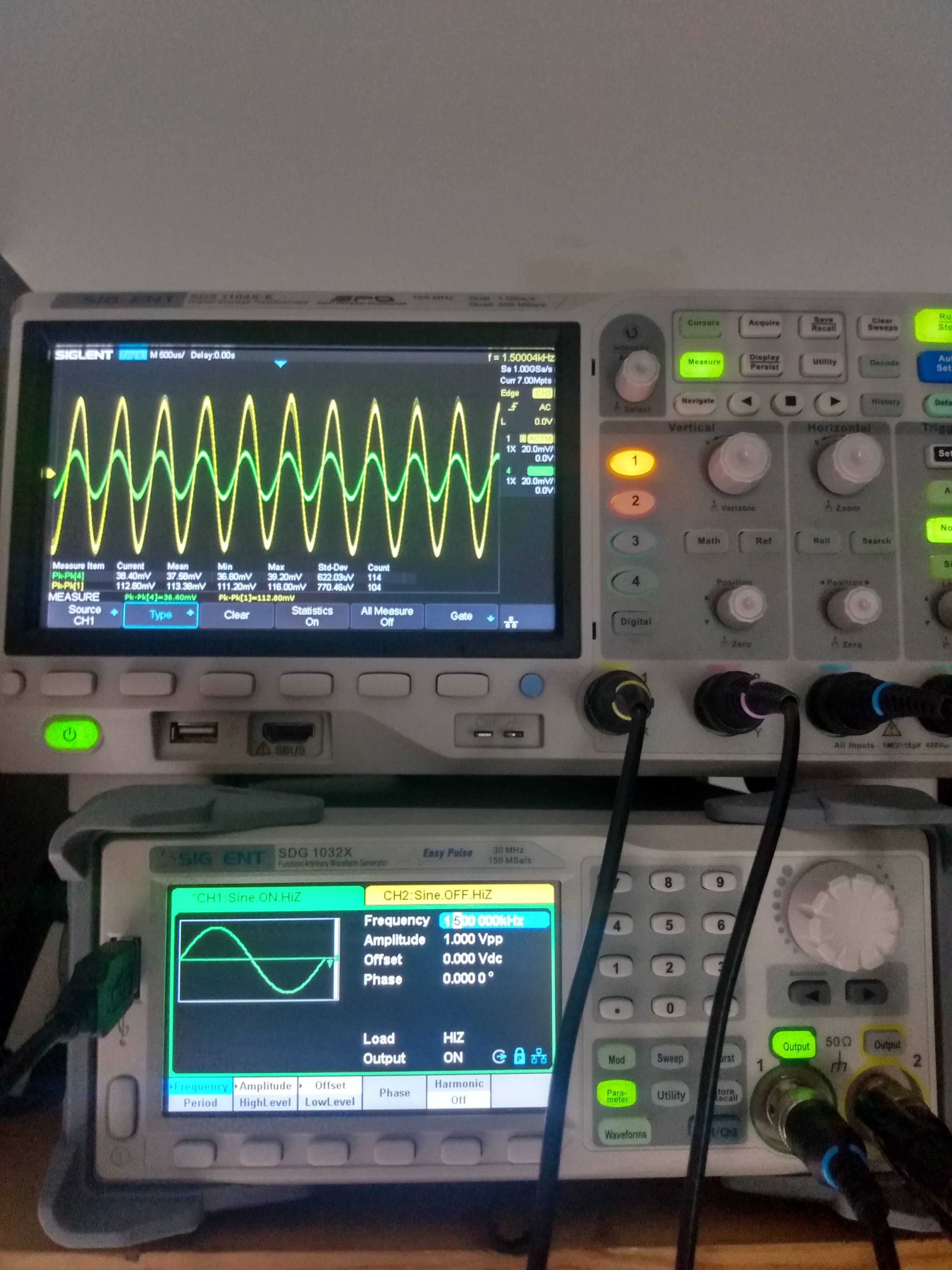
Using my scope I could verify the frame frequency which is equivalent to the sample rate.
I2S
Initially I was hoping to utilize the basic configuration for i2s sound input but I’ve run into a few snags that I’m still trying to troubleshoot. It seems like the default method to record is to configure the I2S port on the Pi as master mode, which conflicts with the PCM1861 trying to drive the signals. In the end I get very odd waveforms which manifests itself as a low voltage threshold of 2V. Troubleshooting is ongoing.
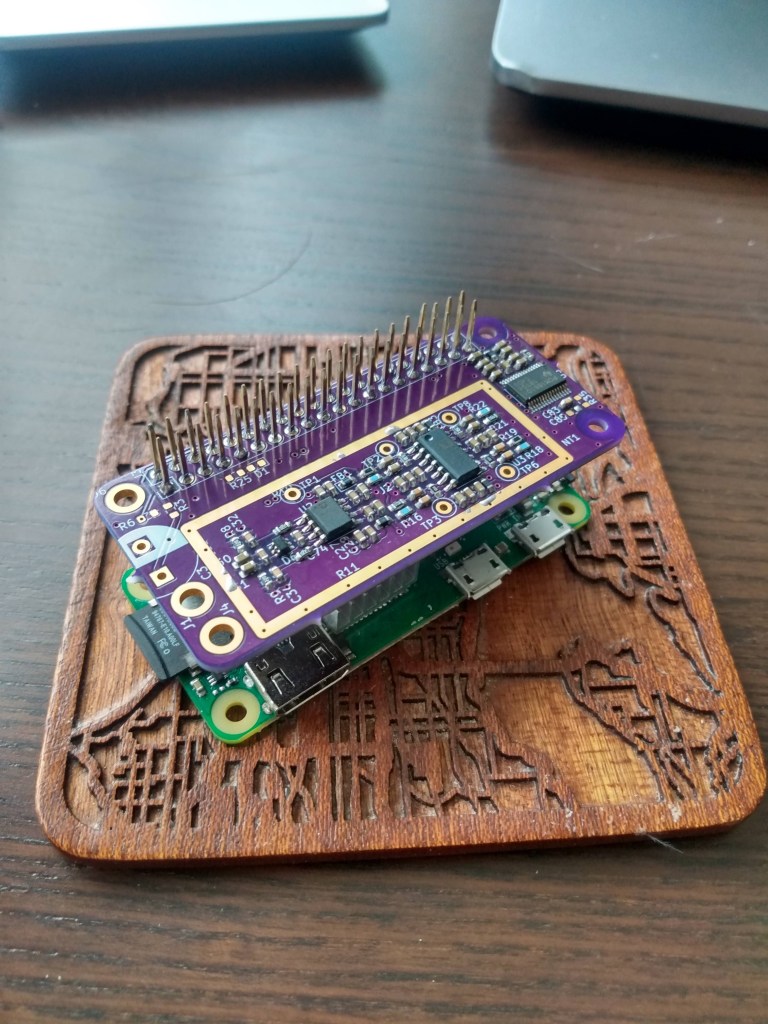
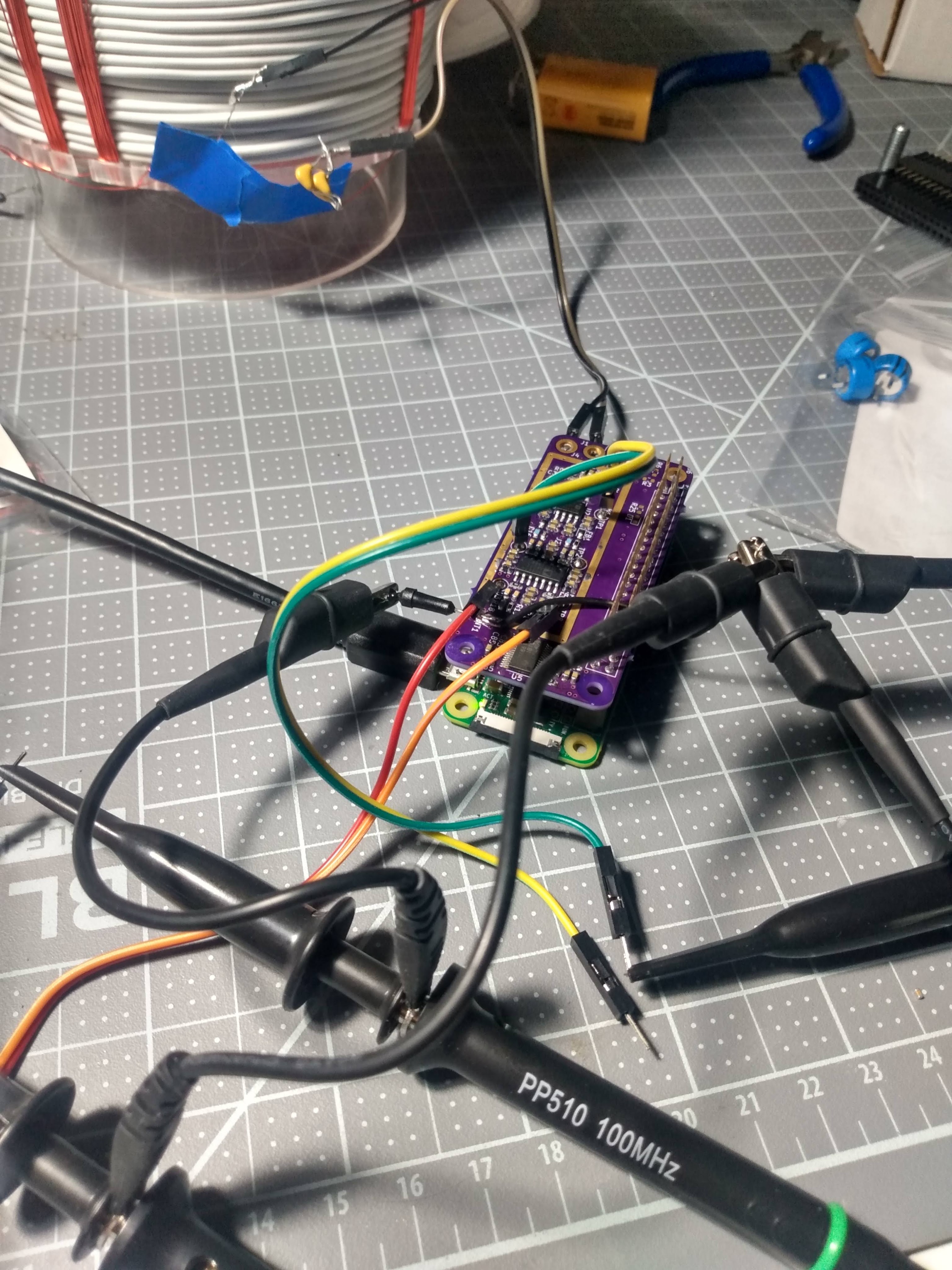
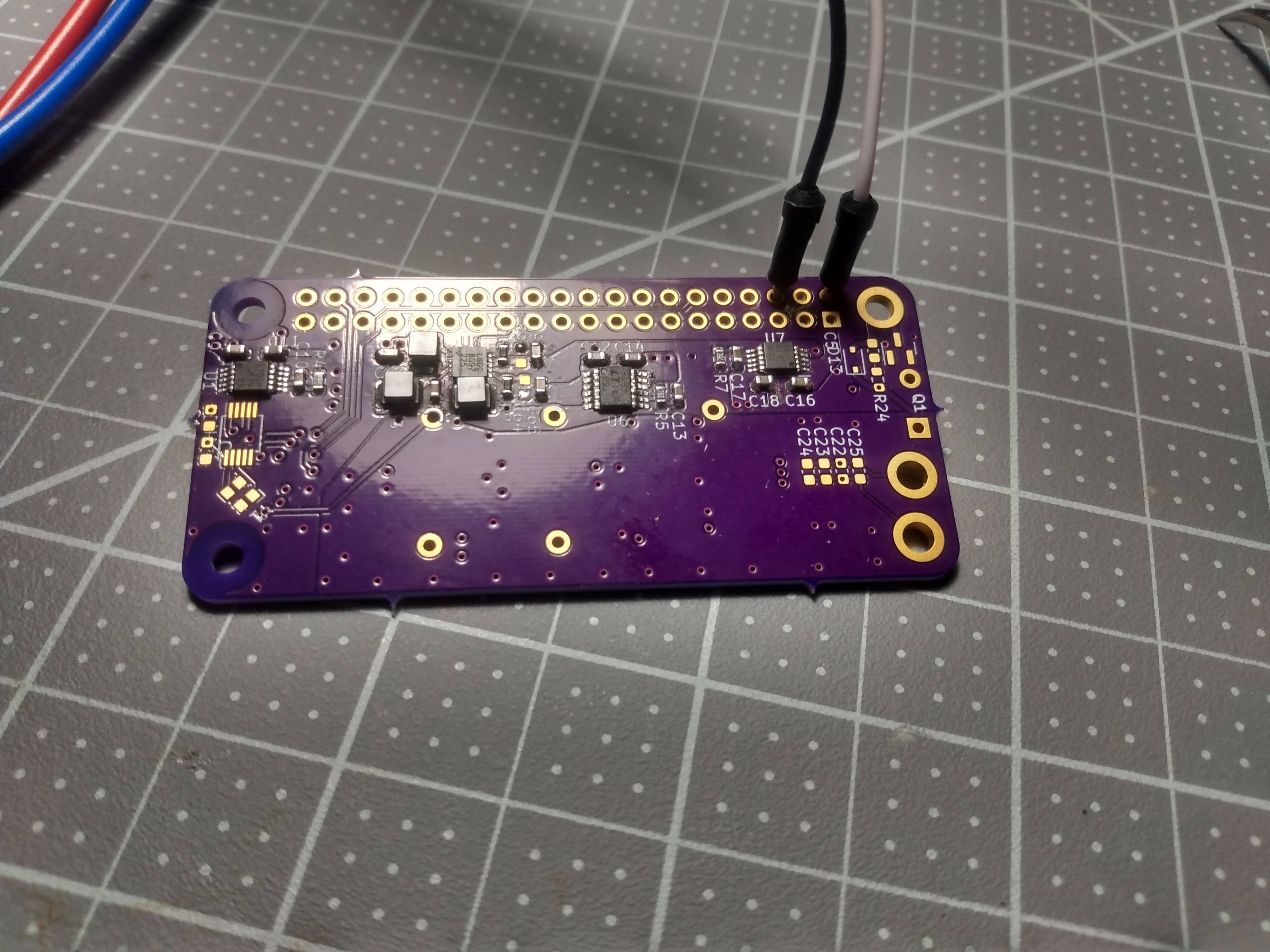
Last week assembly of the power supply stages went without a hitch so this week was spent assembling the remainder of the components. This included the front end module, ADC, and clock generator. Below is a few pictures of the final product.
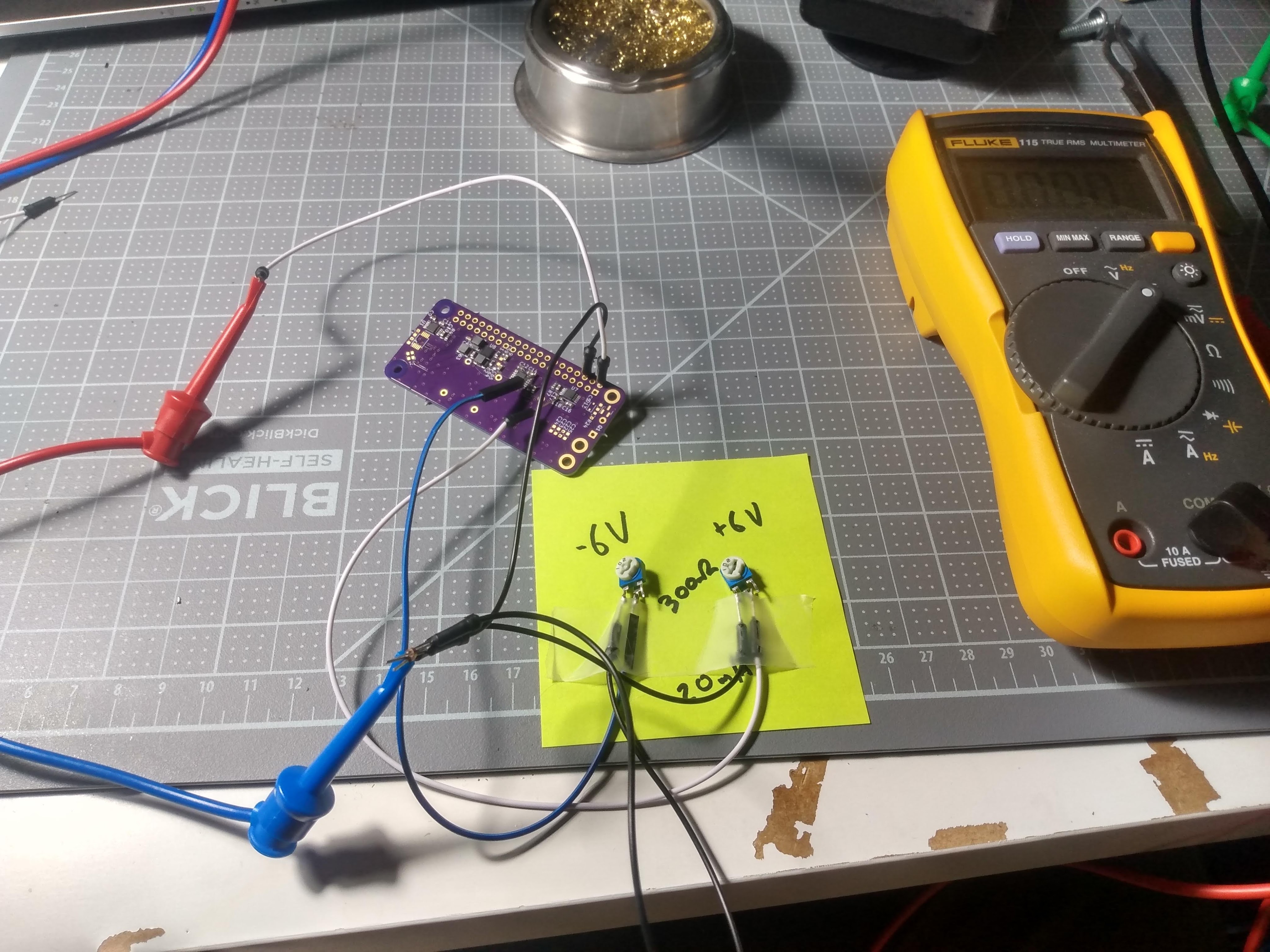
Power Testing
After assembling the board the next step is powering. Always a nerve wracking experience as you never want to hear/see/smell any of the magic smoke escaping. Another layer to my nerves came from the fact that I knew I was pushing my power supply stage near the edge of its performance given the current requirements I had calculated. Fortunately I was conservative in my calculations and the output currents of the amplifier stages is much less than what I had aliquoted.
Final power draw was 150mA @ 5V meaning 750mW. Somewhat higher than I anticipated. Could probably drop this by raising the 2nd stage LDOs closer to the dropout voltage and dissipate less of the headroom.
Front End Testing
Next step was to test out the analog signal change. Jumping the gun a bit I immediately hooked up signal coil. Because if it works right away why go through the baby steps? And the results are in!
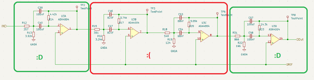
Unfortunately it wasn’t the smashing success that I was hoping for. From the scope measurements it was clear that the 2nd stage 8th order Chebyshev Filter was not doing its job. Measuring at the output of each of the 4 amplifier stage showed very bizarre behavior. Stages 1 and 4 were properly amplifying. Stages 2 and 3 were oddly attenuating the signal.
Root Causing
Sleuthing for the root cause lead me try a variety of things:
Assembly Issue
Simple idea. make sure all the components are properly assembled. The close clustering of the components means silk was a luxury.
Probed all the resistors.
Checked orientation of AD8467 amplifier.
Checked placement of all caps. Can’t probe the caps, but did double check they looked correct.
Component Issue
The original amplifier I was going to use was the ADA4004. However due to the supply chain crisis of Covid-19 I couldn’t get my hands on them so I substituted it with the AD8674 amp. Double checked my assumptions.
Checked pinout.
Checked amp bandwidth.
Checked power supply voltage range.
Power Supply Instability
Maybe the power supplies were unstable and we were operating too close to the edge?
Probe amplifier power rails. No obvious oscillations detectable in the noise floor of my amp (~20mV)
Detach ferrite bead and feed in bench supply. No change in behavior.
ESD issues on amplifier
Hey its an expensive amplifier – probably hates lightning bolts. Swap out component – No change in behavior.
Isolate stage 2 amplifier
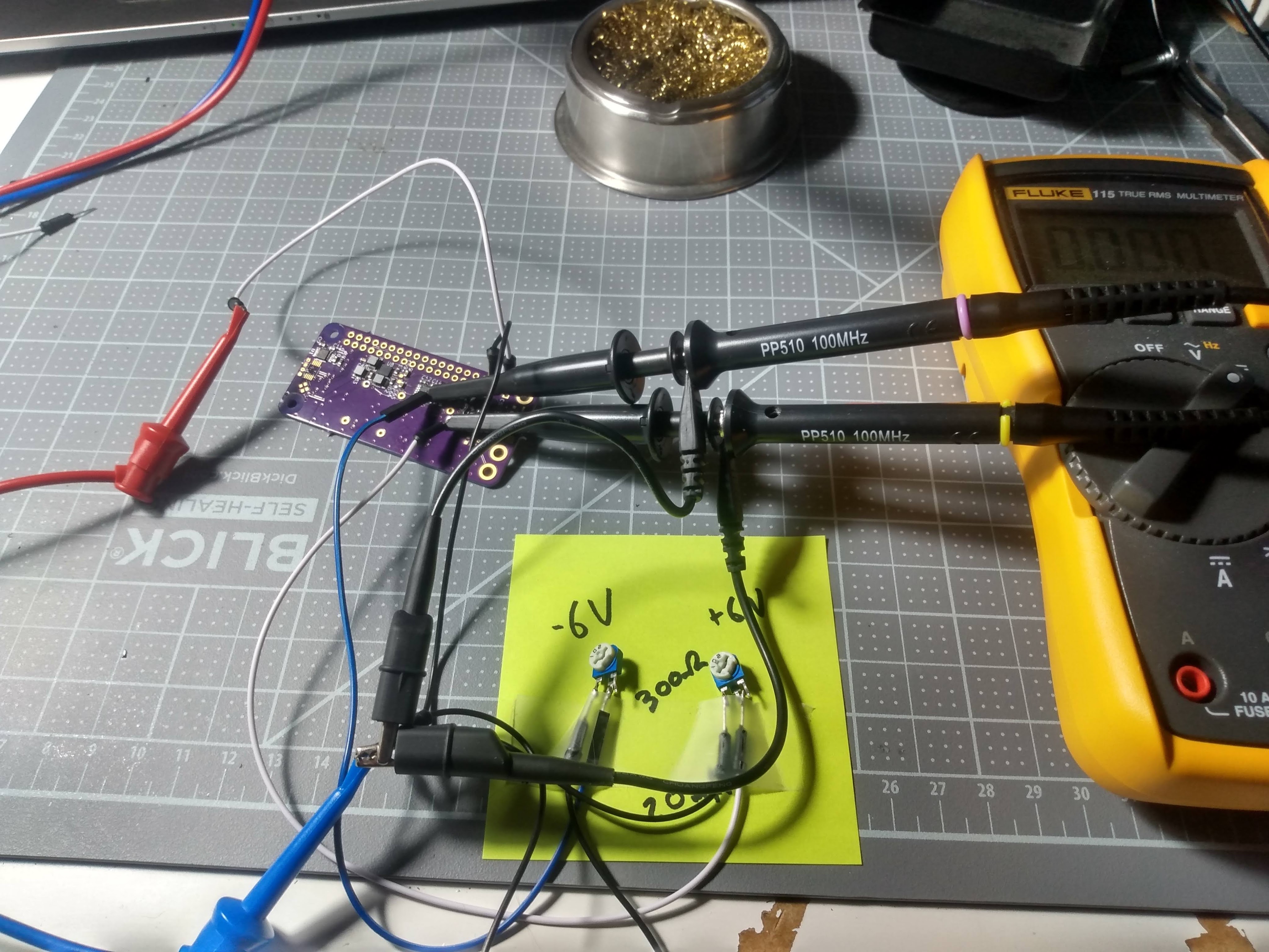
Rather than test out the whole 8th order filter. Isolate stage 2 and see what’s wrong.
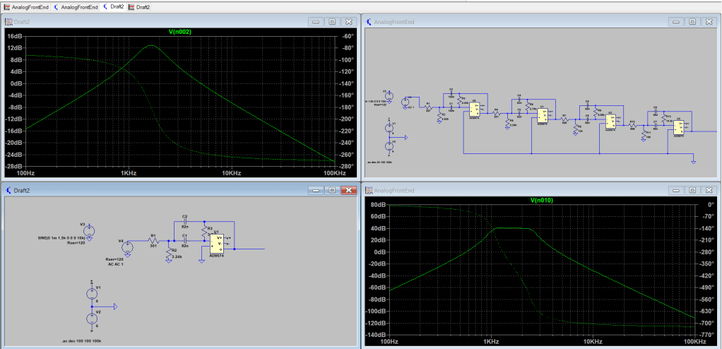
This test was done in conjunction with the isolated power supply. Here I fed in my function generator and probed the output.
Interesting bit of information – The center frequency was ~ 20kHz!! This is a clear indicator as a shift of the center frequency by a decade means there’s a component problem!
In addition to the above I also re-created the filter in LTSpice at step 2. Maybe the behavior was inherent? Below is an image of the response of the filter. My initial simulations were utilizing the ADA4004 so I replaced the model with the AD8674.
With the model and the information that the center frequency was shifted by a decade I experimented with what could cause this. An off by a decade is suspicious of a component order of magnitude error. And naturally when I put in 8.2nF rather than 82nF for stage 2 I found the culprit. I HAD ORDERED THE WRONG CAPACITORS. What a frustratingly simple problem, but glad it wasn’t something more systemic. New caps should arrive sometime this week.
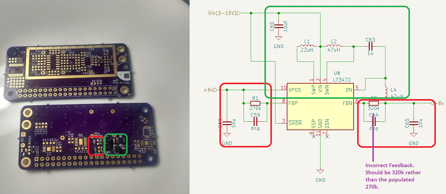
Finally received my new boards from oshpark and started putting together the stage 1 power supply.
Stage 1 is based around the LT3472 and converts the 5V raspberry pi rail into 2 +/- 8 V rail. Noticed an issue when I put it together:
The negative rail was around -6.2V rather than -8V. Looking closer at the datasheet it looks like I misread the equation. Should have set the negative feedback pin to 320k instead of 270k.
Fortunately the Stage 2 drop out voltage of the LT3093 is only around 190mV so there is plenty of headroom between the -6.2V and the final -5V rail.
Did a simple resistive load testing to validate things were still stable up to the expected current draw. The total power draw was a bit higher than expected but wasn’t too crazy to cause too much concern.